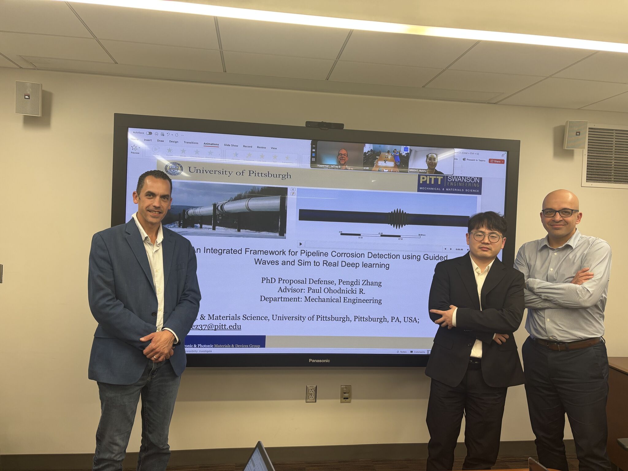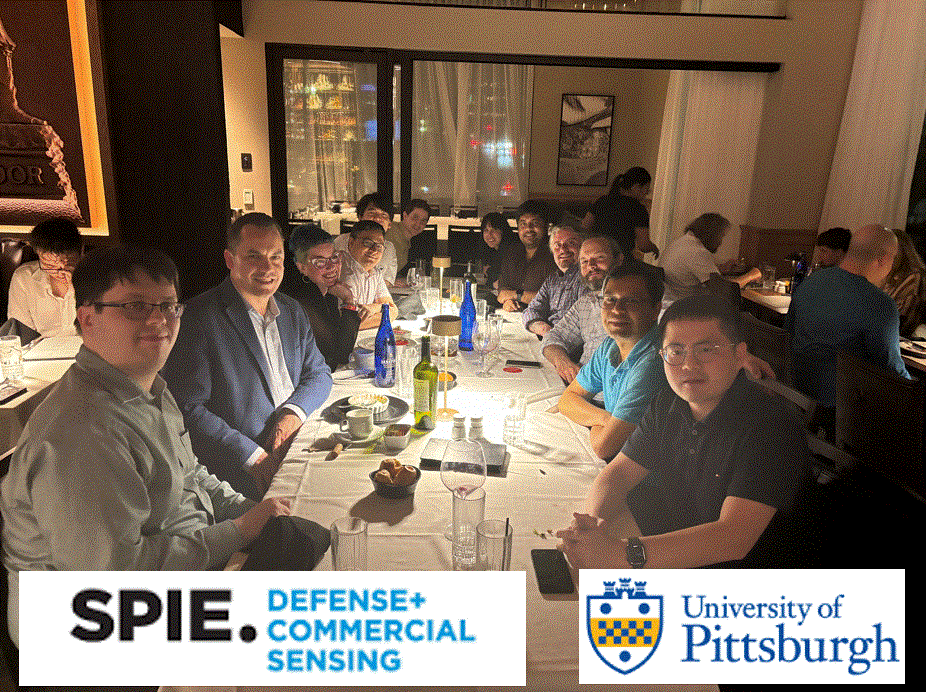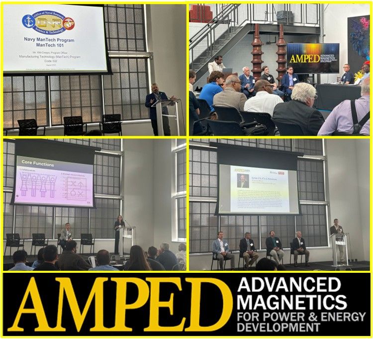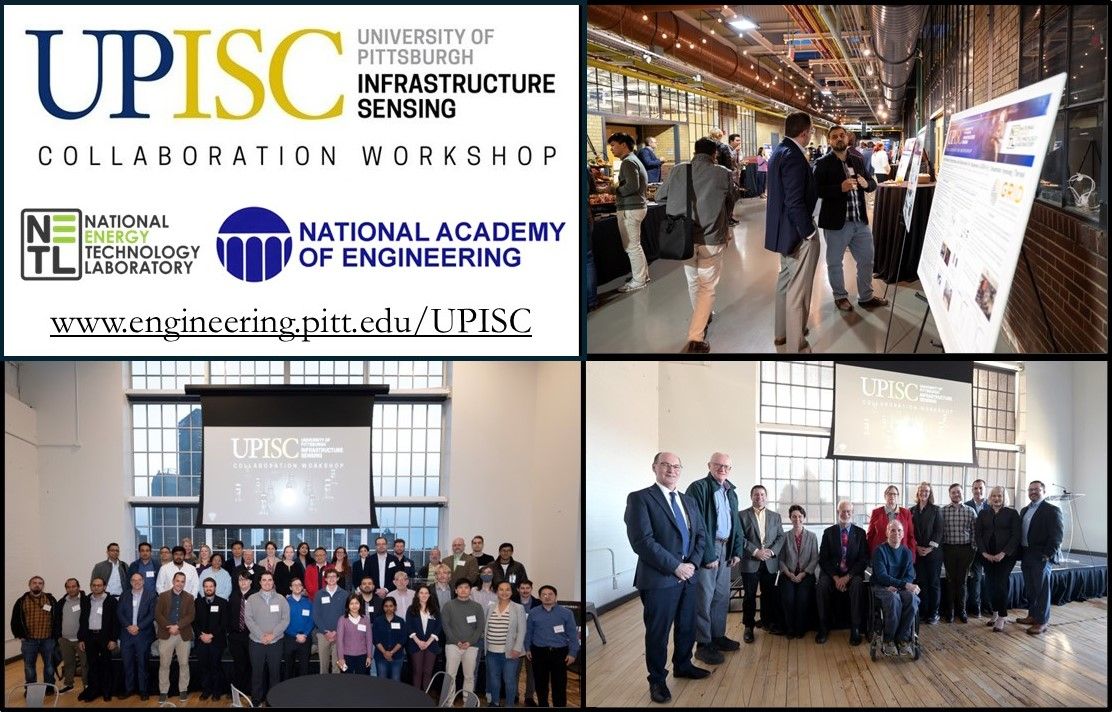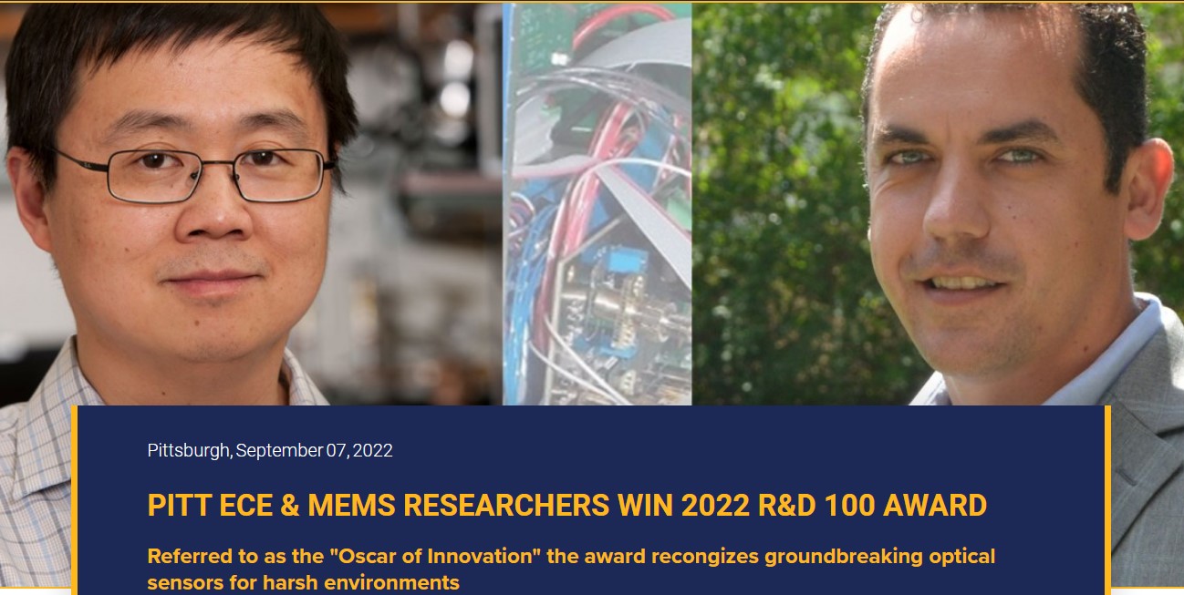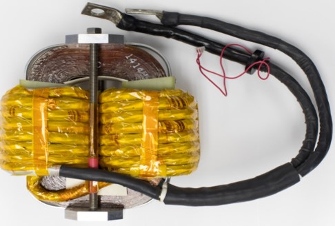
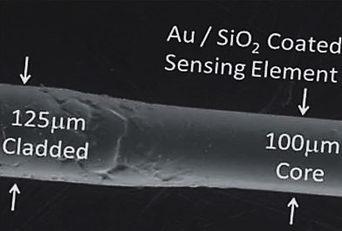
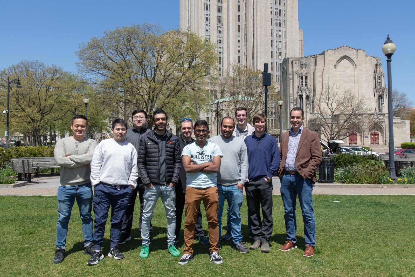
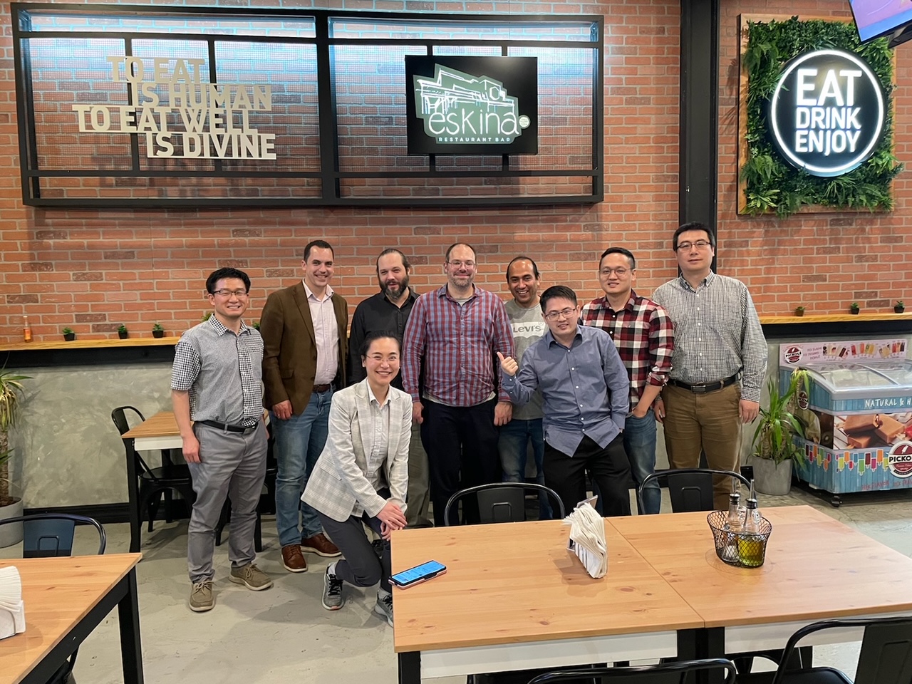

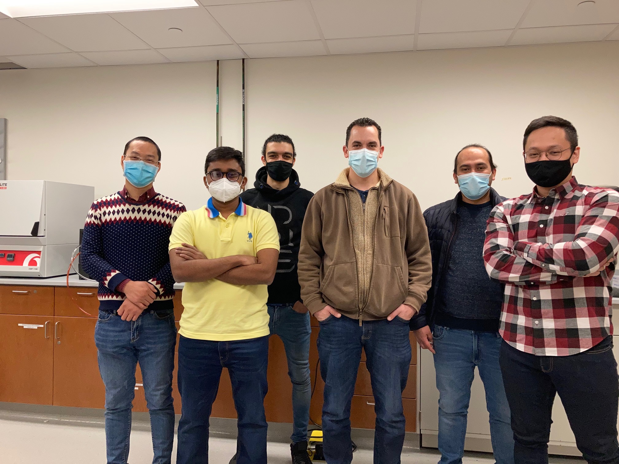
Welcome to Ohodnicki Lab !
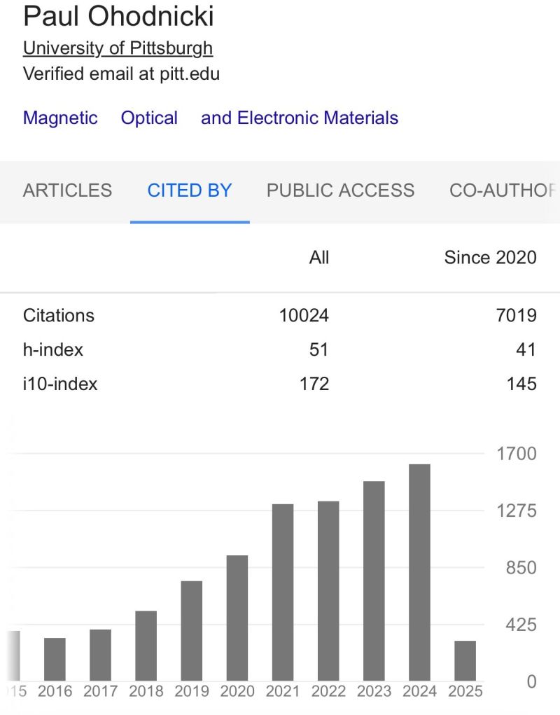
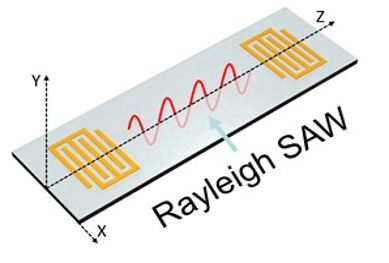
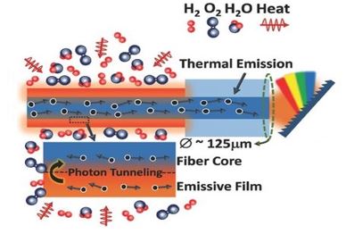
Prof. Paul R. Ohodnicki, Jr. leads the Magnetic, Electronic, and Photonic Materials and Device Laboratory under the Mechanical Engineering and Materials Science Department at the University of Pittsburgh with an emphasis on developing an improved understanding of the interconnection between functional material properties, electronic band structure, and nano/microstructure as well as the optimal integration with emerging device platforms. An early focus of our group is targeting exploration of novel processing methods for emerging high frequency magnetic materials using applied electromagnetic fields spanning the frequency range from DC to optical. Successful pursuit of this research with scientific and technical rigor also requires a detailed understanding of the interplay between electromagnetic fields and emerging material systems under investigation, and so the characterization of material electromagnetic properties over a wide frequency range is also a core capability of the laboratory. Novel photonic and electronic thin film materials are also of interest, including emerging materials with complex electronic band structures such as correlated electron and multi-phase nanocomposite-based systems. Integration of novel functional materials with device platforms is also a core pursuit of the laboratory with applications including optical fiber-based sensors, passive wireless sensors, and inductive components for a wide range of power applications. In all research endeavors, fundamental scientific questions that are pursued and explained have a clear linkage with real-world application needs now or in the future. The Ohodnicki lab was recently started in February of 2020 and is currently in the process of being equipped with a range of instrumentation including: (1) furnaces and ovens for high temperature thermal processing with controlled heating profiles, (2) electromagnetic field assisted thermal processing, (3) high frequency impedance and vector network analyzers with magnetic and dielectric property test fixtures as well as a probe station, (4) automated sensor testing systems, and (5) portable electronic and optical measurement instrumentation. A strong interest exists in tying these capabilities and research endeavors with fundamental and even first principle theoretical calculations to both inform and improve future theoretical modeling efforts as well as to pursue initiatives such as computational design of materials and processing approaches. The laboratory also has an interest in applied electromagnetic modeling methods and techniques to understand the requirements for optimal integration of emerging functional materials systems with device applications.